The MediaTek MT6685 is a 5G module-optimized clock IC system-on-chip with nine clock buffers and four ADC input channels optimized for specific 5G module subsystems.
Provides sophisticated controls for power-up and RTC alarms. The MT6685 is optimized for maximum battery life, allowing the RTC circuit to run for hours without a battery.
The MT6685 uses an SPMI interface and an SRCLKEN control pin to control DCXOs, LDOs, and various drivers; It provides enhanced security controls and protocols for the handshake with the baseband.
The MT6685 is available in a 42-pin WLCSP package. The operating temperature range is -30°C to +85°C.
1. Functional block diagram
The MT6685 is a fully integrated, stand-alone DCXO target for 5G module clock providers. Below is a block diagram of the MT6685 clock IC, see Chapter 5 Application Information for more information.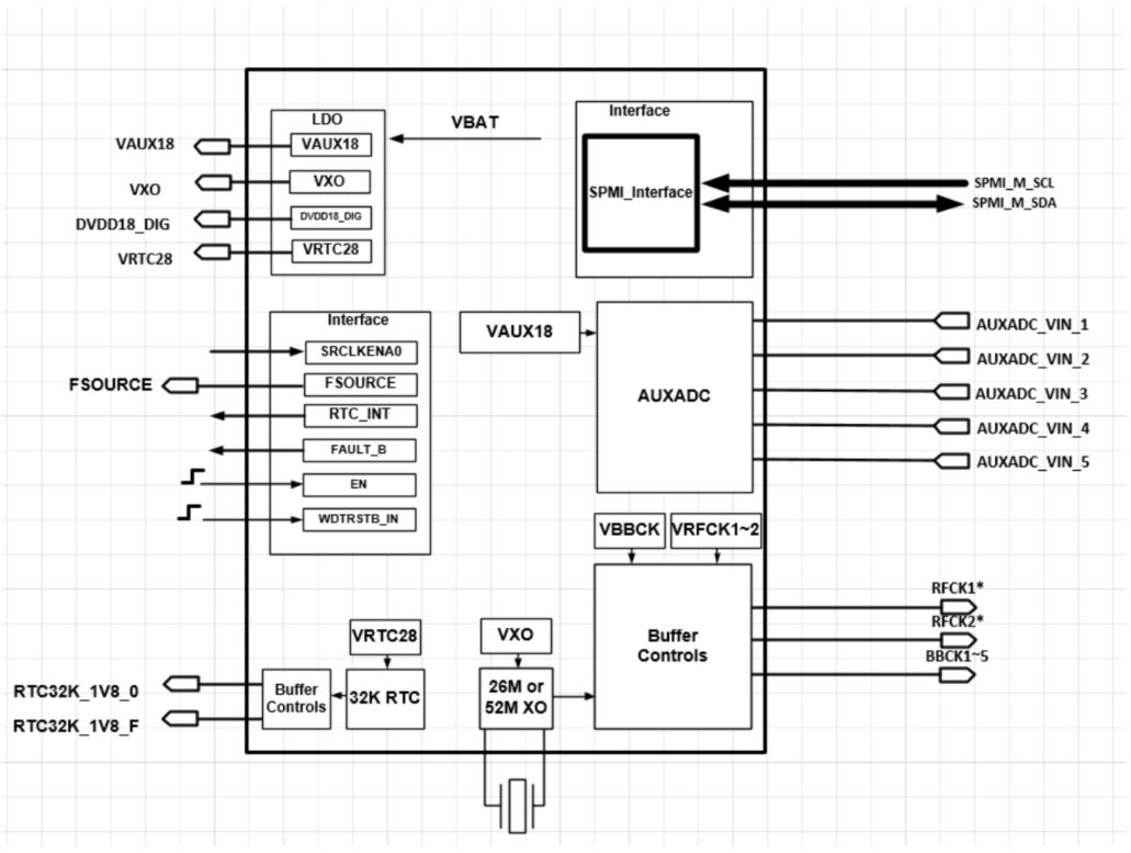
Figure 1-1 Block diagram of MT6685
2. Outstanding features
The MT6685 is ideal for clock ICs for 5G modules and other portable systems.
• Handles baseband clock ICs for 5G modules.
• Input range: 2.6~5V
• 9 clock buffers and 4 ADC input channels optimized for specific 5G module subsystems.
• 32K crystalless RTC oscillator for system timing, 1.8V clock buffer output
• SPMI interface
• Programmable under-voltage lockout protection
• Watchdog reset
• Flexible hardware clock IC reset function
• Power-on reset and start timers
• 42-pin WLCSP package
3. Pin information
3.1 Pin Diagram
Figure 3-1 MT6685 WLCSP 42 (2.2306*2.4958 mm) Pin Assignment (Top View)
3.2 Pin Description
Table 3-1 Pin description of the MT6685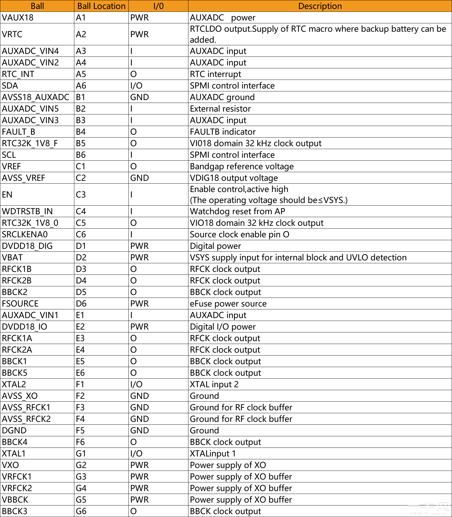
Other

What is HBM (High Bandwidth Memory)?
2024.09.05
What is Antenna Tuner IC?
2024.09.20
What’s the Difference between LPDDR and DDR?
2024.09.25
Snapdragon 888 5G Mobile Platform
2024.09.26

What is WiFi 6E?
2024.09.26
What is Bluetooth Audio SoC?
2024.09.26

What's HBM3E (High Bandwidth Memory 3)?
2024.09.26

What is an Audio Codec?
2024.10.09

