MediaTek MT6833 (see Figure 1-1) integrates Bluetooth, FM, WLAN and GPS modules to create a highly integrated baseband platform that integrates both modem and application processing subsystems for LTE/5G/NR and C2K smartphone applications. The chip integrates two ARM® Cortex-A76 cores operating at up to 2.2 GHz, six ARM® Cortex-A55 cores operating at up to 2.0 GHz, and a powerful multi-standard video decoder. In addition, an extensive set of interfaces and connectivity peripherals are included to connect cameras, touchscreen displays, and UFS/MMC/SD cards.
The application processor is a multi-core ARM® Cortex-A76 and ARM® Cortex-A55 equipped with a NEON engine, providing the necessary processing power to support the latest OpenOS and its demanding applications such as web browsing, email, GPS navigation, and gaming.
All of this is viewed on a high-resolution touchscreen display, and the graphics are enhanced by 2D and 3D graphics acceleration.
Multi-standard video accelerators and advanced audio subsystems are also integrated to deliver advanced multimedia applications and services, such as streaming audio and video, multiple decoders and encoders.
The combination of high-performance CPU, DSP, and hardware coprocessor provides a powerful modem subsystem capable of supporting NR Sub6, LTE Cat 13, Category 24 HSDPA downlink and Category 7 HSUPA uplink data rates, Category 14 TDHSDPA downlink and Category 6 TD-HSUPA uplink, as well as Category 12 GPRS, EDGE.
The MT6833 hardware also embodies Wireless Communication devices, including WLAN, Bluetooth, and GPS. The MT6833 hardware integrates four advanced radio technologies into a single chip, providing the industry's best and most convenient connectivity solution.
Higher overall quality can be achieved when simultaneous voice, data, and audio/video transmission on mobile phones and media tablets. The small footprint and low power consumption greatly reduce the PCB layout resources.
1.1 Highlight features integrated in MT6833 hardware
2 ARM® Cortex-A76 cores operating at 2.2GHz
6 ARM® Cortex-A55 cores operating at 2.0GHz
LPDDR4X up to 12GB (2 lanes, 16-bit data bus width 2 lanes of data bus width)
Memory clocks can reach up to LPDDR4X-4266 Mbps
LTE cat-13 4*4 MIMO
NR Sub6 1CC(MT6833V/ZA)/2CC (MT6833V/NZA)
Embedded connectivity systems, including WLAN/BT/FM/GPS
Resolution up to FHD+ (1,080*2,520)
OpenGL ES 3.2 3D graphics accelerator
ISPs support 32MP@30 fps
HEVC 2,560*1,440@30 fps decoder
HEVC 2,560*1,440@30 fps encoder
Voice codecs (FR, HR, EFR, AMR FR, AMR HR, and wideband AMR and EVS_WB)
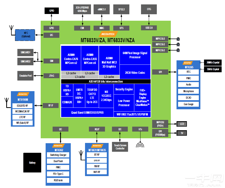
Figure 1-1.High-level MT6833 functional block diagram
1.2 Platform Features
In general
Smartphone, 2 MCU subsystem architectures
Support eMMC/UFS startup
Support LPDDR4X
AP MCU subsystem
2 ARM® 2.2 GHz Cortex-A76 cores, each with 64 KB L1 I-cache, 64 KB L1 Dcache. The kernel has 64KB L1 I-Cache, 64KB L1 Dcache, and 256KB L2 Cache
6 ARM® 2.0 GHz Cortex-A55 cores, each with 32 KB L1 I-cache and 256 KB L2 cache. The cores have 32KB L1 I-cache, 32KB L1 Dcache, and 128KB L2 cache
Shared 1MB of L3 cache
NEON multimedia processing engine with support for SIMDv2/VFPv4 ISA
DVFS technology with adaptive operating voltages from 0.55V to 0.973V
MD MCU subsystem
High-performance multi-core and multi-threaded processor architecture
High-performance AXI bus interface
A general-purpose DMA engine and a dedicated DMA channel for peripheral data transfer
Power management for clock gating
MD external interface
Dual SIM/USIM interfaces
RF and radio-related interface pins Interface pins for peripherals (antenna tuners, PAs, etc.).
security
ARM® TrustZone® security
External memory interface
LPDDR4X, up to 12GB (2 channels, 16-bit data bus width Data bus width).
Memory clocks can be up to LPDDR4X-4266
Self-refreshing/partially self-refreshing mode
Low-power operation
Programmable Memory Slew Rate Programmable slew rate for the controller's I/O pads
Dual-grade memory devices
Advanced bandwidth quorum control
Peripherals
USB2.0 OTG
eMMC5.1
UFS2.2
2 UARTs for debugging and application
8 SPI masters for external devices
4 I2Cs/6 I3Cs to control peripherals.
For example: CMOS image sensors, LCM or FM receiver modules
Utmost. 4 PWM channels (depending on system configuration/IO usage) Maximum 4 PWM channels (depending on system configuration/IO usage).
I2S for connecting an optional external Hiend audio codec
GPIO
2 sets of memory card controllers, supporting SD/SDHC/MS/MSPRO/MMC and SDIO2.0/3.0 protocols
working conditions
Core voltage: 0.55~0.725V
I/O voltage: 1.8V/2.8V/3.3V
Memorizer. 0.8V
LCM interface. 1.8V
Clock source: 26MHz, 32.768kHz
encapsulation
Type. VFBGA
12.05mm*12.05mm
Height. Utmost. 0.9 mm
The number of balls. 888 balls
Ball spacing: 0.35mm
1.3 Modem Functions
NR
3GPP EN-DC Option 3/3a/3x
3GPP SA Option 2
FDD/TDD up to 2.77 Gbps downlink, 1.25 Gbps uplink
Support 5~100MHz RF bandwidth per component carrier (CC) RF bandwidth
Supports SCS 15/30 kHz
Supports downlink/uplink 256QAM
Supports 4*4 MIMO on the downlink and 2*2 MIMO on the uplink
LTE is supported
FDD/TDD downlinks up to 391 Mbps and uplinks up to 150 Mbps uplinks
Downlink Carrier Aggregation (CA) capability.
RF bandwidth of 1.4~20MHz per component carrier (CC) and up to 2 CC
Inband Carrier Aggregation (CA) for Uplinks
Ability; Each component carrier (CC) has an RF bandwidth of 1.4~20MHz, and can have up to 2 CC.
Component carrier (CC) and RF bandwidth of up to 2 CC
DL 256 QAM/UL 64 QAM is supported
4*2 downlink SU-MIMO carriers for each component
Downlink MU-MIMO for each component carrier
MBMS is supported
Uplink CoMP capability
Advanced interference cancellation
▪ PDCCH pIRC
CRS-based PDSCH
DMRS-based Co-UE
Transmitting antenna selection
Features supported by 3G UMTS FDD
3G modems support most of the main features of 3GPP versions 7 and 8
CPC (DTX IN CELL_DCH, UL DRX DL DRX), HSSCCH-, HS-DSCH-. Less, HS-DSCH
Two-unit operation
MAC-ehs
2 DRX (Receiver Diversity) schemes, 2 DRX (Receive Diversity) schemes in URA_PCH and CELL_PCH
Uplink Cat. 7 (16 QAM) with a throughput of up to 11.5 Mbps
Downlink Cat. 24 (64 QAM, two-cell HSDPA). Throughput up to 42.2 Mbps
Rapid hibernation
ETWS
Network selection enhancements
Transmitting antenna selection
TD-SCDMA
CDMA/HSDPA/HSUPA baseband
TD-SCDMA 34, 39, 40 and quad-band GSM/EDGE
circuit-switched voice and data; Packet-switched data
TD-SCDMA has a UL/384Kbps rating in the DL
TD-HSDPA: 2.8 Mbps DL (Cat.14)
TD-HSUPA: 2.2 Mbps UL (Cat.6)
F8/F9 encryption/integrity protection
Transmitting antenna selection
Radio interface and baseband front-end
IQ data (DigRF) via a high-speed serial interface is carried out between the RF and the baseband chip.
Programmable radio Rx filter with adaptive gain control
Dedicated Rx filter for FB acquisition
Baseband Parallel Interface (BPI) and MIPI Programmable-Driven RFFE Interface Benefits
Multi-band support
GSM modem and voice codec
Dial tone generation
Noise reduction
Echo suppression
Advanced sidetone oscillation reduction
Digital sidetone generator with programmable gain
Other
What is HBM (High Bandwidth Memory)?
2024.09.05
What is Antenna Tuner IC?
2024.09.20
What’s the Difference between LPDDR and DDR?
2024.09.25
Snapdragon 888 5G Mobile Platform
2024.09.26
What is WiFi 6E?
2024.09.26
What is Bluetooth Audio SoC?
2024.09.26
What's HBM3E (High Bandwidth Memory 3)?
2024.09.26

What is an Audio Codec?
2024.10.09

