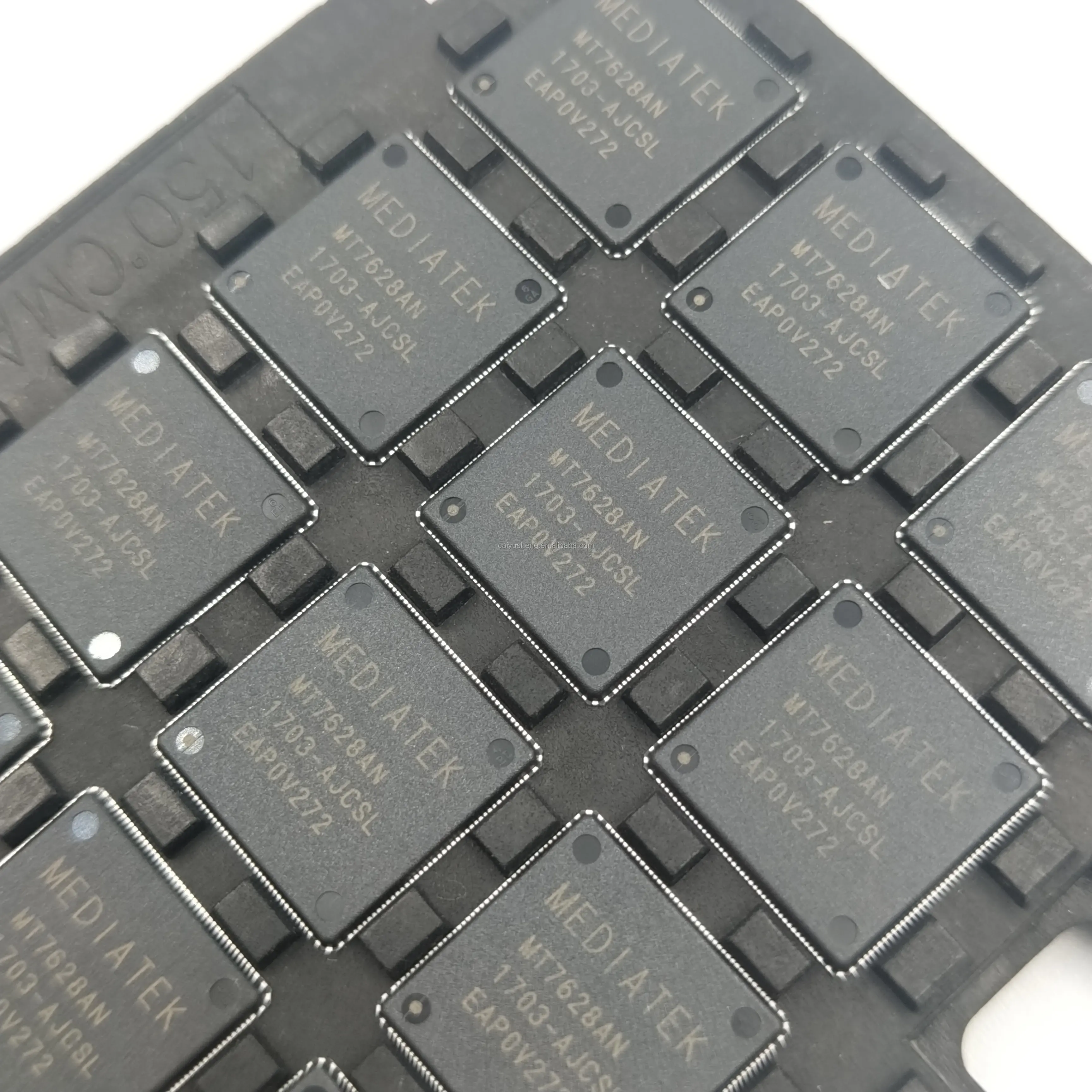
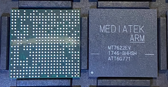
Product Description
The MediaTek MT6315RP/B is a highly integrated power management IC (PMIC) designed to meet the demanding power requirements of modern mobile devices. Its architecture is tailored to provide efficient power distribution and management, which is crucial for maintaining optimal performance while extending battery life.
One of the standout features of the MT6315RP/B is its ability to support a wide input voltage range, making it versatile for various applications. The configurable output voltage options allow designers to customize the power supply according to the specific needs of the device, whether it be a smartphone, tablet, or wearable technology. This flexibility is particularly beneficial in a market where device specifications can vary significantly.
The efficiency of the MT6315RP/B is another critical aspect. With efficiencies reaching up to 95%, the chip minimizes power loss, which is essential for battery-operated devices. This high efficiency is achieved through advanced voltage regulation techniques, including synchronous rectification and low-dropout regulation, which ensure that the device operates effectively under different load conditions.
Thermal management is also a key consideration in the design of the MT6315RP/B. The chip incorporates thermal protection features that prevent overheating, thereby enhancing the reliability and longevity of the device. This is particularly important in compact devices where space constraints can lead to increased heat generation.
In terms of integration, the MT6315RP/B reduces the need for multiple discrete components, which simplifies the overall design and can lead to cost savings in manufacturing. The compact QFN package allows for easy placement on printed circuit boards (PCBs), making it an attractive option for device manufacturers looking to optimize space without compromising on performance.
Overall, the MediaTek MT6315RP/B is a robust and efficient power management solution that addresses the challenges of modern mobile device design. Its combination of high efficiency, flexible output options, and integrated protection features make it a valuable component in the development of next-generation consumer electronics.
Specification
Input Voltage Range: 3.0V to 5.5V
Output Voltage Options: Configurable from 1.0V to 3.3V
Output Current: Up to 1A per channel
Efficiency: Up to 95% under typical load conditions
Operating Temperature Range: -40°C to +85°C
Package Type: QFN (Quad Flat No-lead) package, typically 4mm x 4mm
Number of Outputs: Multiple outputs (typically 4-6), depending on the specific configuration
Control Interface: I2C or similar digital control interface for configuration and monitoring
Protection Features: Over-current protection, thermal shutdown, and under-voltage lockout

